New Technology / Gpu
Unclear topic
ASML's DUV technology remains crucial in chip production, accounting for a significant portion of the manufacturing process.
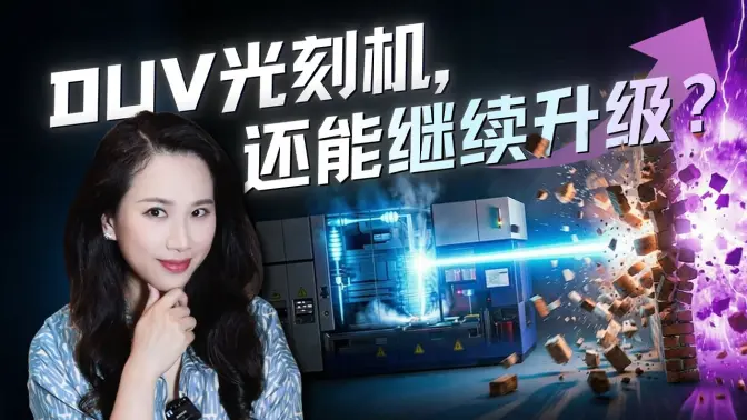
Source material: It's 2026, why is ASML still researching the 'previous generation' DUV? [Silicon Valley 101]
Summary
ASML's DUV technology remains crucial in chip production, accounting for a significant portion of the manufacturing process.
Despite advancements in EUV technology, DUV machines are more efficient and cost-effective for many applications.
ASML continues to innovate within the DUV space to enhance production capabilities and meet market demands.
The integration of DUV technology with advanced lithography solutions creates a positive feedback loop in chip manufacturing.
Perspectives
Focus on the significance of DUV technology in the semiconductor industry.
Support for DUV Technology
- Emphasizes DUVs role in producing 90% of advanced chips
- Highlights DUVs cost-effectiveness compared to EUV
- Points out DUVs efficiency in handling multiple chip layers
Advocacy for EUV Technology
- Argues for the potential of EUV to revolutionize chip manufacturing
- Raises concerns about the long-term viability of DUV as technology evolves
Neutral / Shared
- Acknowledges the ongoing innovation in DUV technology
- Recognizes the importance of balancing DUV and EUV in production
- Notes the challenges associated with 3D chip integration
Metrics
production_efficiency
400.0 units
DUV machine exposure rate
Higher exposure rates lead to increased production efficiency.
This is the highest output DUV lithography, capable of exposing over 400 wafers per hour.
production_efficiency
220.0 units
EUV machine exposure rate
Lower exposure rates in EUV machines limit their production capacity.
This is currently the highest output EUV lithography, exposing up to 220 wafers per hour.
market_share
90.0 %
DUV's share in advanced chip production
A significant market share indicates DUV's critical role in chip manufacturing.
DUV's performance can even reach ninety percent.
exposure_area
4.0 units
exposure area of the ThingsGAN XT 260 compared to traditional machines
This increase in exposure area can significantly reduce production time and costs.
Provides four times the market of traditional methods
throughput
400.0 units
wafers produced per hour
Higher throughput indicates improved efficiency in chip manufacturing.
Can increase the output of sutras to over 400 pieces in less than an hour.
Key entities
Timeline highlights
00:00–05:00
The production of advanced three-nanometer chips still heavily relies on older DUV machines, which account for up to 90% of chip manufacturing. Despite the introduction of EUV technology, DUV remains essential due to its cost-effectiveness and efficiency in producing various chip layers.
- Most of the latest three-nanometer chips in smartphones are still produced using older DUV machines, highlighting the ongoing relevance of DUV in chip manufacturing
- ASMLs DUV machines produce the majority of chips globally, including those made with EUV technology, as even the most advanced chips rely on DUV for many of their layers
- DUV remains the dominant technology in chip production, accounting for up to 90% of advanced chip manufacturing, indicating its continued importance in the mainstream market
- The production cost is a significant factor preventing a complete shift to EUV, as DUV machines can expose over 400 wafers per hour compared to the 220 wafers of the most efficient EUV machines
- Many chips, such as automotive and memory chips, prioritize cost and stability over extreme precision, further solidifying DUVs position in the market
- There is still potential for innovation in DUV technology, especially with the shift towards 3D chip stacking, which allows for vertical growth in chip design
05:00–10:00
3D integration in chip manufacturing involves stacking multiple chips vertically, which presents challenges such as alignment precision and structural stability. ASML's innovations, including the ThingsGAN XT 260 lithography machine, aim to enhance production efficiency and accuracy in this complex process.
- 3D integration in chip manufacturing involves stacking multiple chips vertically, presenting challenges such as alignment precision and structural stability. ASML optimizes lithography processes to facilitate this integration, focusing on the K1 factor for improvements
- Overlay accuracy is critical for the alignment of multi-layer chips, and enhancements can be achieved through stable materials and optimized processes. ASML has established a department dedicated to achieving high flatness in lithography equipment, essential for precise imaging
- ASMLs ThingsGAN XT 260 lithography machine is designed for advanced packaging, offering significant improvements in exposure capabilities. It provides four times the exposure area compared to traditional machines, reducing the need for stitching and enhancing production efficiency
10:00–15:00
ASML's acquisition of Hermes Microwation in 2016 for approximately 2.75 billion euros has proven beneficial for their lithography solutions. The core requirements in chip mass production include precise measurement and rapid inspection to ensure quality and performance.
- In 2016, ASML acquired Hermes Microwation for approximately 2.75 billion euros, a deal that was 30% above the market price at the time, proving beneficial as it became a crucial part of their holistic lithography solution
- The core requirements in chip mass production are measurement and inspection, with measurement focusing on precise values and inspection quickly scanning for physical defects
- To enhance overlay accuracy, ASML employs a feedback loop where measurement data from previous layers dynamically adjusts exposure parameters for subsequent layers, similar to a marksman adjusting their aim
- ASML has transitioned from optical inspection tools to electron beam inspection tools for higher precision, although the latter are slower than optical methods
- ASML is upgrading electron beam inspection tools to improve detection speed, which is crucial for maintaining efficiency in chip manufacturing
- In 2D microfabrication, the challenges of DUV technology are increasing as circuit sizes shrink, prompting the adoption of new design techniques to enhance transistor density
15:00–20:00
ASML's Tunescan NXP870B has improved throughput to over 400 wafers per hour, enhancing production efficiency. The company continues to invest in DUV technology to meet market demand and improve precision in chip production.
- ASMLs latest Tunescan NXP870B has upgraded optical components, increasing throughput to over 400 wafers per hour, significantly enhancing production efficiency
- The integration of computational lithography and metrology tools creates a positive feedback loop, optimizing chip manufacturing processes
- ASML continues to invest in DUV technology due to persistent market demand and its ability to improve both precision and throughput in chip production
- DUV technology supports 3D integration by enhancing precision and contributes to economic efficiency through increased production yields
- ASMLs strategy involves a dual approach where the DUV route safeguards chip production while the EUV route explores future lithography advancements